
 Contact us
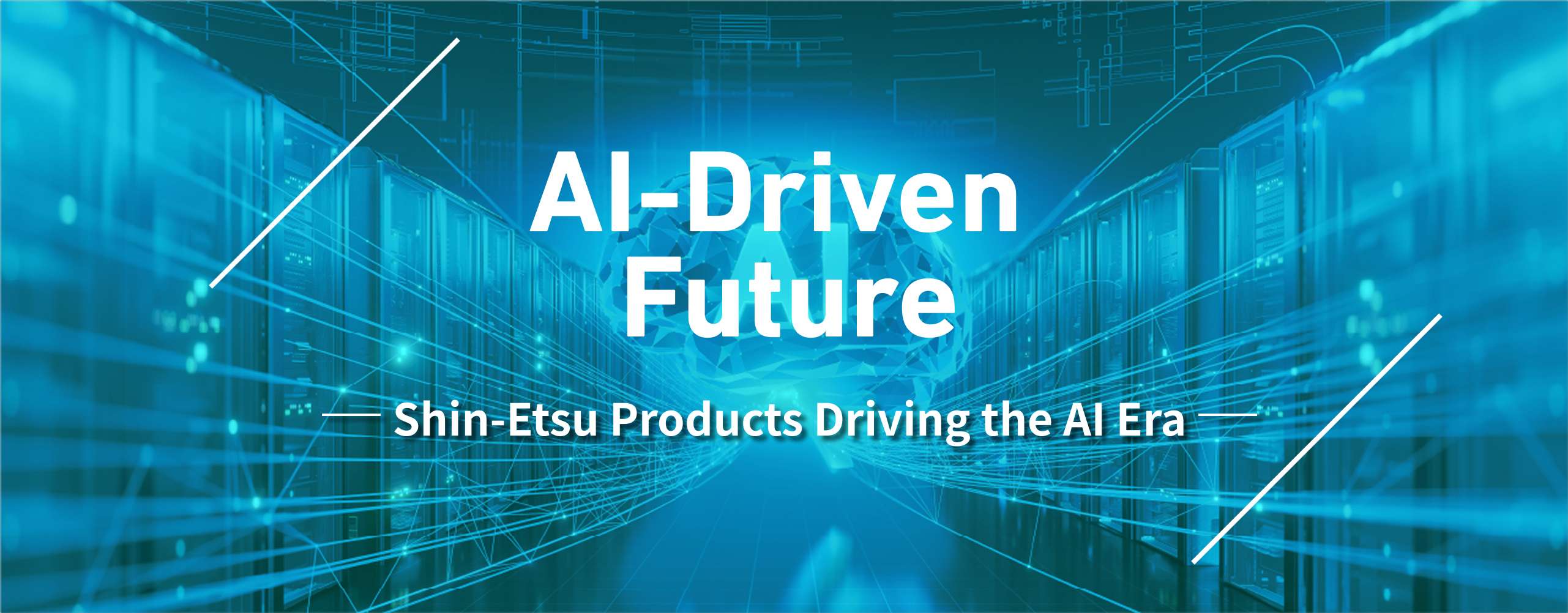
AI-Driven Future: Shin-Etsu Products Driving the AI Era
- Home > Sustainability >
- Products supporting the cutting edge of AI semiconductor manufacturing and use
- Accelerating the evolution of AI through the development and innovation of diverse materials
- Advancing into the next generation through integration of manufacturing, sales, and R&D
-
Employee Interviews
- #01 Immersion Cooling: The superior properties of immersion cooling silicone contribute to energy and resource conservation in data centers
- #02 Thermal Interface Materials: Silicone heat-dissipation materials that reduce environmental impact and support the stable operation of AI
- #03 QST™substrate: Developing next-generation power semiconductors that significantly reduce data center power demand
Since the advent of generative AI, the real-world deployment of AI has accelerated across industries and society. With the development of physical AI, which uses AI to operate robots, automobiles, drones, and other devices, it is predicted that AI will increasingly become an infrastructure technology for industry and daily life going forward. On the other hand, challenges have emerged in scaling AI in the real-world, including growing electricity demand. As AI semiconductors are pushed to deliver ever-higher performance, their energy requirements continue to rise, driving a sharp increase in data center electricity use.
Against this backdrop, utilizing AI as social infrastructure will require further improvements in the AI chip performance efficiency, reductions in data center power consumption, greater efficiency in communications and enhanced energy savings across application areas such as automobiles and robotics.
The Shin-Etsu Group not only holds the world's leading market share in silicon wafers (single-crystal silicon), which serve as the substrates for all AI semiconductors, but also supplies materials necessary for manufacturing processes such as semiconductor circuit patterning and molding materials to protect chips. We are also engaged in the development and manufacture of a wide range of materials that contribute to creating an environment needed to maximize AI performance, including materials for cooling semiconductor chips and servers, building systems for storage and optical communications. Through this diverse product portfolio, we contribute not only to various technological innovations in AI semiconductors, but also to energy savings and the efficient use of resources in AI deployment environments, including data centers.
The Shin-Etsu Group's major AI-related products
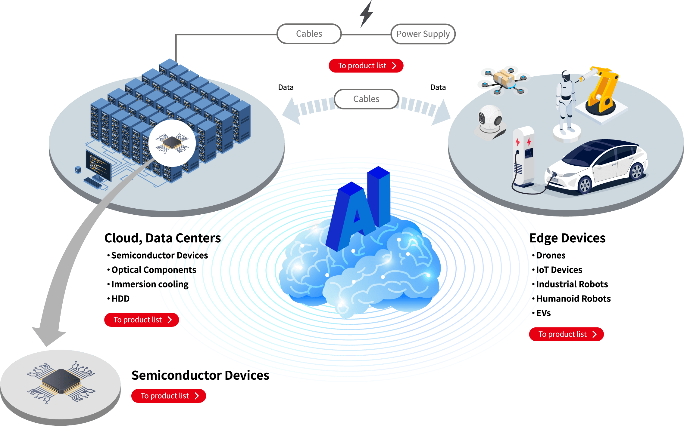

e.g.) Silicon Wafers, Photoresist etc.


e.g.) Silicon Wafers, Photoresist etc.
To improve the data processing capabilities of AI semiconductors, the process node has been reduced to a few nanometers*1 in the cutting edge devices. In terms of memory, new technologies continue to emerge, including HBM*2, which stacks multiple layers of DRAM*3. The Shin-Etsu Group contributes to improving the efficiency of AI semiconductors by providing the highest quality silicon wafers, as well as a wide range of materials to meet the advanced needs of semiconductor manufacturing processes, including high-purity deposition gases essential for circuit formation, photoresists necessary for circuit pattern formation, photomask blanks that serve as circuit pattern masters, pellicles that act as dustproofing films, and TBDB materials indispensable for the manufacturing of advanced semiconductors. In addition, we further contribute to improving the efficiency of AI semiconductors through the development of new materials. As increasing chip power consumption makes heat dissipation ever more critical, we provide effective thermal management solutions through silicone-based thermal interface material (TIM)*4.
Nevertheless, the power consumption for cooling in data centers is said to have already reached about 40% of the facility's total power consumption. As data centers continue to handle ever-larger volumes of data at higher speed, there is a growing demand for more effective cooling systems, and the adoption of cooling systems using highly electrically insulating liquids (immersion cooling) is beginning to gain momentum. Shin-Etsu Chemical is promoting the practical deployment of an immersion cooling system using silicone fluid with low environmental impact. This non-fluorine-based (non-PFAS*5) silicone fluid is highly stable and suitable for long-term use. The technology contributes to making data centers more energy-efficient while helping to conserve resources.
In the field of power semiconductors, which are essential for controlling power supply, we are working to develop wafers optimized for the growth of gallium nitride (GaN), which is attracting attention as a key next-generation material. Through these efforts, the Company aims to help address the challenge of significantly reducing the power consumption at data centers.
*11 Nanometer:
One millionth of a millimeter
*2HBM (High Bandwidth Memory):
A type of semiconductor memory that consists of multiple DRAM chips stacked on top of each other, enabling high-speed processing of massive amounts of data.
*3DRAM (Dynamic Random Access Memory):
A type of semiconductor memory commonly used as the main memory in PCs and smartphones.
*4TIM (Thermal Interface Material):
A material that fills the gap between heat-generating components such as AI chips and heat dissipation components such as heat sinks, effectively dissipating heat.
*5PFAS:
Collective term for perfluoroalkyl compounds and polyfluoroalkyl compounds.
Today, driven by advances in AI semiconductors, development and proof-of-concept validation are progressing in optoelectronic integration, a next-generation technology that aims to achieve faster data processing and lower power consumption with the goal of extending the domain of optical signal processing. Shin-Etsu Chemical stably supplies high-quality SOI wafers*, which are expected to be used in such next-generation technologies. In addition, we are advancing the development of optical fiber preforms that deliver the properties required for next-generation platforms, as well as materials for optical modulators, which are key components in optoelectronic integration. The Shin-Etsu Group integrates manufacturing, sales, and R&D to ensure that it stays ahead of changes in social and market needs. We will continue to contribute to the realization of a sustainable society through the stable supply of products that support a wide range of industries and everyday life, including the field of AI.
*SOI (Silicon on Insulator):
A composite wafer in which a thin film of silicon is bonded onto an insulating layer on a silicon substrate.
#01
Immersion Cooling
The superior properties of
immersion cooling silicone
contribute to energy and
resource conservation in
data centers
Read the interview
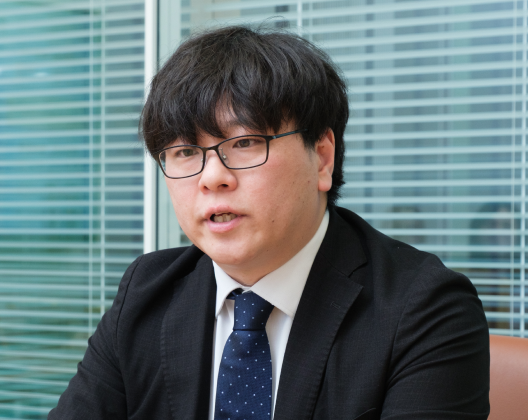
 S.I., Fluid Group, Sales and Marketing Department I ,
Silicone Division
S.F., 1st Development Department,
Silicone-Electronics Materials Research Center
Cooling the server by fully submerging it
Advantages of being able to tailor characteristics to customer requirements
A future in which we can contribute to local communities and families
#02
Thermal Interface
Materials
Silicone heat-dissipation
materials that reduce
environmental impact
and
support the stable
operation of AI
Read the interview
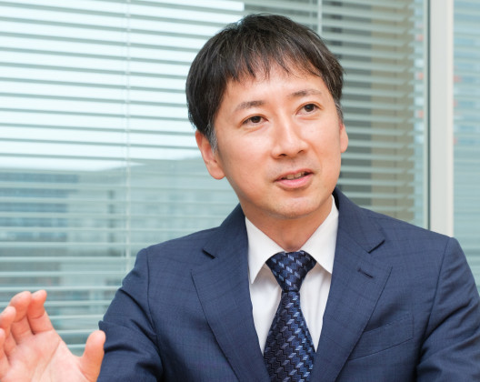
 K.T., Senior Researcher,
2nd Development Department,
Silicone-Electronics Research Center
S.A., Product Development Group,
Sales and Marketing Department Ⅲ,
Silicone Division
Heat dissipation materials are essential for the stable operation of AI
One of silicone's advantages is the high degree of freedom it brings to product design
Contributing to curbing ever-increasing power consumption
*Main chain
The core silicone backbone formed by alternating silicon and oxygen atoms, known as the siloxane bond. A key feature of silicone is that bonding various organic groups to its main chain allows it to be given a wide range of properties.
#03
QST™substrate
Developing next-generation
power semiconductors that
significantly reduce data
center power demand
Read the interview
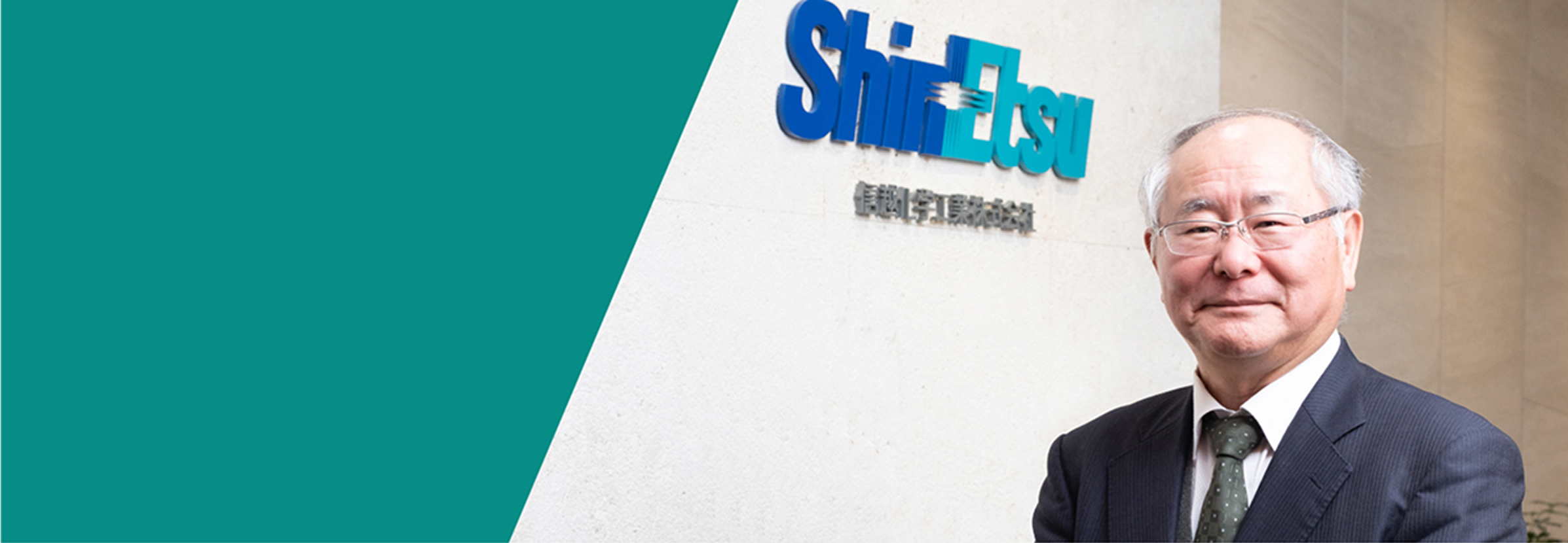 M.Y., Manager, Shin-Etsu Chemical GaN Commercializing Unit
Establishing the fundamental technology for QST™ substrate for GaN epitaxial growth
As AI becomes widespread, reducing the power consumption of the AI data centers that support it has become a major challenge. According to estimates by the International Energy Agency (IEA), worldwide electric power demand for data centers reached 415 terawatt-hours in 2024 and is expected to reach 945 terawatt-hours by 2030, exceeding the total electricity consumption of Japan as a whole. To curb this enormous demand for electricity, innovation in power semiconductors is urgently needed. Power semiconductors are devices that perform roles such as converting the high-voltage alternating current supplied to data centers into direct current, converting voltage levels, and controlling frequency. They are used in many places throughout the data center, from its power receiving infrastructure to the power supply for the servers that serve as its brain. There are therefore high expectations for the improved performance of power semiconductors to solve challenges such as reducing the electrical energy lost as heat.
Shin-Etsu Chemical is focusing on gallium nitride (GaN) as a next-generation material for these power semiconductors. In 2019, we signed a licensing agreement with Qromis, Inc. in the United States, and began full-scale development of QST™* substrate for GaN epitaxial growth. GaN is expected to offer excellent properties, such as reducing electrical energy and contributing to the miniaturization of devices, but until now it has been difficult to create substrates that can fully realize these characteristics. To overcome this challenge, we incorporated our own proprietary technologies to suppress the occurrence of defects, enabled the manufacture of large-diameter wafers, work to enable the use of silicon carbide (SiC) and GaN as "higher-performance seed crystals" for power semiconductors. We have even made it possible to recycle the base substrate. As a result, power semiconductors using this technology can withstand high-voltage loads of up to 1200V, making them usable in the power receiving infrastructure of data centers, while also reducing energy loss by more than 80% compared to conventional devices. Furthermore, by enabling the miniaturization of power supply components and reducing the need for heat dissipation, power consumption for cooling and other related processes can be reduced, dramatically lowering the overall power demand of the AI data center. Moreover, recycling can reduce the electricity required for conventional crystal substrate manufacturing and lower the consumption of gallium (Ga), one of the rare materials.
Partnerships with Group companies and customers
The foundational technologies for these next-generation power semiconductors are built on the technologies and expertise in compound semiconductor manufacturing that Shin Etsu Chemical has cultivated over many years. I myself have experience in the development and sales of compound semiconductors used in LEDs and other applications, and that experience has been helpful in the development of QST™ substrate. Furthermore, the cooperation of device manufacturers is essential for gathering information on customer needs and for technical verification. In this regard, our group company Shin-Etsu Handotai Co., Ltd. and our global network have been a great help. Since we are primarily a material manufacturer, we need to rely on device manufacturers and global R&D institutions to evaluate the performance of the devices incorporating our materials. We have also been conducting performance evaluations of the newly developed QST™ substrate with the cooperation of device manufacturers and research institutions that are our customers. After receiving positive feedback in 2025, we became convinced that even the large-diameter 300 mm wafers that were previously considered difficult could be commercialized.
We were this time able to make great use of our existing partnerships with our customers in the compound semiconductor field. When we spoke to OKI Electric, with whom we have had a relationship on compound semiconductors for LEDs, about recycling QST™ substrate that forms the base of GAN devices, we discovered that the company's CFB® technology could be utilized, and joint development is now underway for the real-world deployment of GaN devices. I believe that this recycling process will significantly reduce the energy and materials required for substrate manufacturing and will also allow us to make better use of valuable Ga resources by eliminating the need for GaN substrates.

Greater focus on real-world deployment
QST™ substrate has only just reached the stage where the fundamental technology is established, and there will still be many hurdles to overcome before they can be adopted as power devices worldwide. However, we have a foundation of overcoming obstacles through partnerships with our customers, and with the support from Shin-Etsu Group companies around the world, I am confident that we can clear these hurdles and deliver innovation.
*QST™
Abbreviation for Qromis Substrate Technology, a gallium nitride (GaN) technology patented by Qromis, Inc. in the United States. By incorporating its proprietary technologies, Shin-Etsu Chemical has further improved the properties of the original QST™ substrate—for example, by suppressing defects and cracking to enable larger-diameter substrates —and is now developing second- and third-generation substrates.
Related Information