
 Contact us
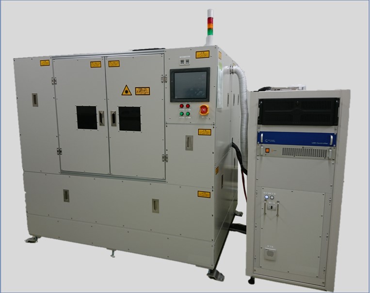
LASER debonding equipment
LASER peeling equipment, laser irradiation equipment
LASER debonding equipment
This LASER debonding equipment is used for a semiconductor packaging process or manufacturing process for ultra-thin semiconductors to peel off a temporary bonding layer with a LASER beam without stress.
Using a pulse LASER with a LASER beam wavelength of 355 nm licensed from IBM, this equipment ensures that the LASER beam is absorbed only on the surface of a temporary resin layer, thus curtailing damage to the device.
It supports FOPLP of large panel size, achieving uniform LASER irradiation for workpieces of up to 600 mm2.
-
Company:Shin-Etsu Engineering Co., LTD.
-
Department:Electro-Mechanics Division
-
Email:systeminfo@see.jp