
 Contact us
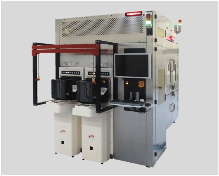
X-ray bump/void inspection equipment
X-ray inspection equipment, bump inspection equipment, X-ray observation equipment, solder inspection equipment
X-ray bump/void inspection equipment
Equipment to inspect/judge bumps on the wafer automatically.
By transmitting X-rays through voids (air bubbles) inside the wafer, the void diameter (area) is calculated from a transmitted image to automatically judge whether to accept voids exceeding standards.
It uses a microfocus X-ray tube as an X-ray source, and a cutting-edge X-ray digital camera for the X-ray image receiving section, to extract high-resolution images and enable high-precision void inspection.
Series Name
Applications
-
Company:Shin-Etsu Engineering Co., LTD.
-
Department:Electro-Mechanics Division
-
Email:systeminfo@see.jp