
 Contact us
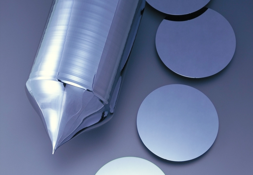
Silicon Wafers
Semiconductor silicon
Silicon Wafers
High purity silica rocks, which can be found only in select mines around the world, are reduced to silicon metal in a special furnace. From this silicon metal, polycrystalline silicon of 99.999999999% purity is created, and this is the raw material used by Shin-Etsu to fabricate semiconductor grade single-crystal silicon wafers. Special crystal growing methods are used to melt polycrystalline silicon and then convert to a large single-crystal round ingot, having perfect atomic structure. These crystals can be 300mm in diameter and longer than one meter. A silicon wafer is produced by slicing these ingots, followed by shaping and polishing processes. The final silicon wafer, which has extremely low levels of contamination and defects and surface particles is the “substrate” used to create many types of semiconductor devices, which are the foundation for the world around us. Silicon wafers are the primary substrate for the devices which power our smartphones, personal computers, digital home appliances, and which are now leading to remarkable advances in autonomous automobiles, AI, robotics, and healthcare.
Series Name
Applications
-
Company:Shin-Etsu Chemical Co., Ltd.
-
Department:Semiconductor Materials Dept.
-
Phone:+81-3-3246-5211