
 Contact us
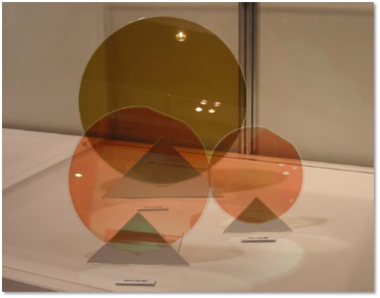
Hybrid wafers
Hybrid wafers
Hybrid wafer is a combination of active and functional layers such as GaN, SiC, LT or LN and the base substrates that have a basic desirable properties such as Si, AlN, Si3N4 or quartz, which is manufactured by our original bonding technologies.
We provide substrates suitable for RF, power devices for IOT, 5G, and in-vehicle devices.
Click here to download the PDF.
Applications
-
Company:Shin-Etsu Chemical Co., Ltd.
-
Department:Advanced Functional Materials Research Center
-
Email:hybrid_sub@shinetsu.jp