Compound semiconductor ingot and wafer
| Shin-Etsu handoutai (SEH) supply the compound semiconductor ingot and various wafer (bulk and epitaxial wafer). We have a track record of supplying various As and P-based substrates. |
Ingot and wafer line up
| Ingot and Bare wafer | Epitaxial wafer |
|---|---|
| GaP(gallium phosphide) | HVPE epitaxial wafer(GaP base) |
| MOVPE epitaxial wafer(GaAs,InP base) | |
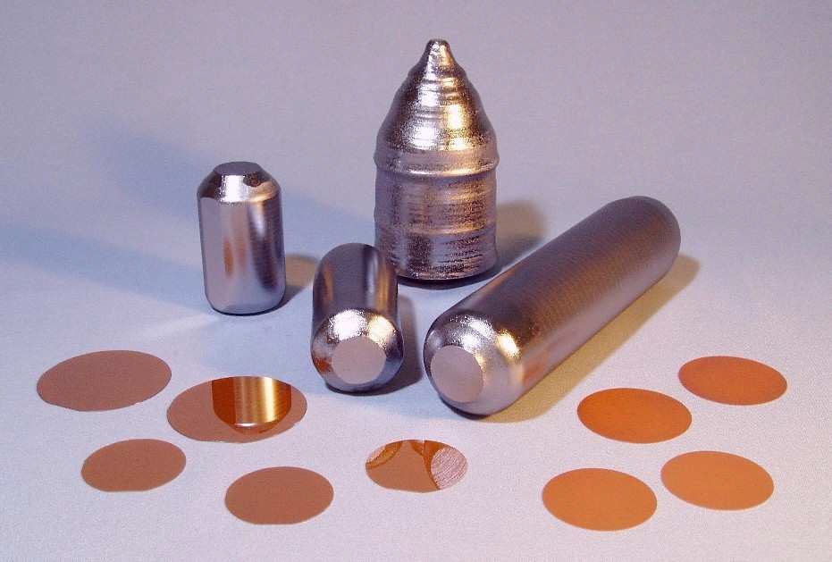 |  |
Ingot GaP
(gallium phosphide)
Bare wafer of GaP
(gallium phosphide)
| Based orientation is (100). Please contact us if you would like to need other orientation. |
PAGE TOP
HVPE epitaxial wafer
| We have a track record of growing GaN using the HVPE method. Please contact us if you would like to grow GaN. |
PAGE TOP
MOVPE epitaxial wafer
| Please contact us if you would like to manufacture with other materials. It is possible to manufacture epitaxial wafers using materials with P and/or As materials. |